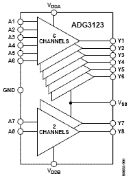
The ADG3123 is an 8-channel, noninverting CMOS to high voltage
level translator
DESCRIPTION
The internal architecture of the device ensures compatibility with logic
circuits running from supply voltages within the 2.3 V to 5.5 V range.
The voltages applied to Pin VDDA, Pin VDDB, and Pin VSS set the
logic levels available at the outputs on the Y side of the device. Pin
VDDA and Pin VDDB set the high output level for Pin Y1 to Pin Y6
and for Pin Y7 to Pin Y8, respectively. The VSS pin sets the low output
level for all channels. The ADG3123 can provide output voltages levels
down to −10 V for a low input level and up to +30 V for a high input
logic level. For proper operation, VDDB must always be greater than or
equal to VDDA and the voltage between the Pin VDDB and Pin VSS
should not exceed 35 V.
FEATURES
- 2.3 V to 5.5 V input voltage range
- Output voltage levels (VDDA and VDDB to VSS ≤ 35 V)
Low output voltage levels: down to −24.4 V
High output voltage levels: up to +35 V
- Rise/fall time: 12 ns/19.5 ns typical
- Propagation delay: 80 ns typical
- Operating frequency: 100 kHz typical
- Ultralow quiescent current: 65 μA typical
- 20-lead, Pb-free, TSSOP package
Subscribe to:
Post Comments (Atom)
0 comments:
Post a Comment